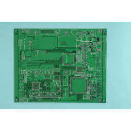
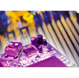
*Multilayer: 4 to 12 layers high-density various material PCBs *Material: FR-4, 0.5 to 3oz copper, 0.15 to 3.2mm thickness *Minimum line width and line spacing: 4mm *Minimum hole diameter: 0.2mm *Maximum panel size: 480 x 580mm *Surface finishing: *HAL. alpha level, gold plating, ENTECH *HAL or tin and gold plating *Solder mask type: photo liquid *Precision V-cut for panel form design *OEM orders for SMT and A/I assembly projects accepted *Gerber file preferred *Please note the following information are for your reference on our manufacturing capability, not for inquiries on quotes *We will offer our best prices if you can send us your own PCB design
*Multilayer: 4 to 12 layers high-density various material PCBs *Material: FR-4, 0.5 to 3oz copper, 0.15 to 3.2mm thickness *Minimum line width and line spacing: 4mm *Minimum hole diameter: 0.2mm *Max
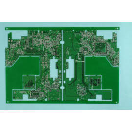
*Multilayer high density various material PCBs *Material: FR-4 or CEM-3,0.5 to 3oz copper, 3.2mm thickness *Minimum line width and line spacing: 4mm/4mm *Minimum hole diameter: 0.2mm *Max panel size:
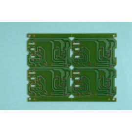
*Double side high density various material PCBs *Material: FR-4 or CEM-3,0.5 to 3oz copper, 3.2mm thickness *Minimum line width and line spacing: 4mm/4mm *Minimum hole diameter: 0.2mm *Max panel size
*Double side high density various material PCBs *Material: FR-4 or CEM-3,0.5 to 3oz copper, 3.2mm thickness *Minimum line width and line spacing: 4mm/4mm *Minimum hole diameter: 0.2mm *Max panel size
*Double side high density various material PCBs *Material: FR-4 or CEM-3,0.5 to 3oz copper, 3.2mm thickness *Minimum line width and line spacing: 4mm/4mm *Minimum hole diameter: 0.2mm *Max panel size


 help
help Add to favorite
 Favorite products