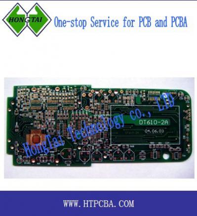
PCB process capability Base material: CM1, CM3, FR1, FR4, Metal based Layer: 1 to 24 layers Board thickness: 0.4mm to 3mm Copper thickness: 0.5oZ, 1oZ, 2oZ Min Copper thickness in hole: 0.02mm Max working size: 400*610mm Surface finishing: HASL, OSP, Immersion Gold Min drill hole size: 0.2mm Min line width/space: 0.1mm PCB shape treatment: V-cut, Routing, Punching Solder Mask color: white, black, green, blue, red and so on Production capacity of PCB: 8000 square meters per month Production capacity of PCBA: 100,000pcs per month
PCB process capability Base material: CM1, CM3, FR1, FR4, Metal based Layer: 1 to 24 layers Board thickness: 0.4mm to 3mm Copper thickness: 0.5oZ, 1oZ, 2oZ Min Copper thickness in hole: 0.02mm M
PCB process capability Base material: CM1, CM3, FR1, FR4, Metal based Layer: 1 to 24 layers Board thickness: 0.4mm to 3mm Copper thickness: 0.5oZ, 1oZ, 2oZ Min Copper thickness in hole: 0.02mm M
Likewise in category "Electronic Component Networks":


 help
help Add to favorite
 Favorite products